A Field Programmable Gate Array (FPGA) is a device that is user configurable by using a binary image file to implement the required functionality. The main focus for these devices has been digital centric designs although some FPGAs have tried to address other areas by inclusion of analogue blocks and other Intellectual Property (IP) blocks.
An Application Specific Integrated Circuit (ASIC) is a custom designed integrated circuit that is dedicated for one particular application. Both digital and analogue functions can be implemented and with a wide array of process choices available some power functionality is also possible.
Both are used extensively in product designs and which path to take is a conundrum that designers are often faced with. It’s an important decision that can determine the products success or failure, and unfortunately there is not a definitive answer. It is only by examining each solution for each design with up to date information that a designer can make the appropriate selection.
Consider the whole life cycle
Each solution has advantages and disadvantages, which have different relevance dependent on where you are in a products life cycle. If you do not consider the full life cycle there is a danger that you can make the wrong decision.
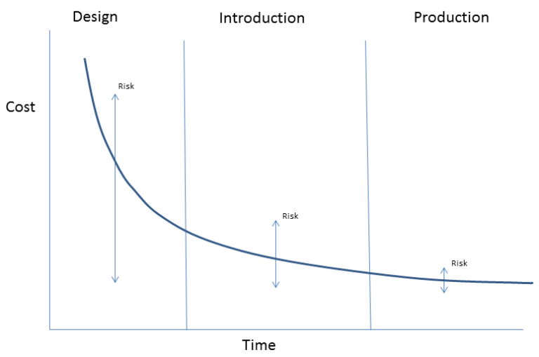
A further complication is that the latter stages of the product life cycle are often based on forecasts, which can make designers more cautious and lead to a wrong selection and hence higher costs. A typical product life cycle is shown below.

Design and Development
Whilst in the development phase of a project there is only expenditure with no returns so keeping this to a minimum is desirable. It is worth noting that FPGA and ASIC digital development will look very similar in the early stages, i.e. system and block design, partitioning and system modelling are common activities.
Analogue design requirements makes the difference
It is only as the design progresses that there is a divergence. Any analogue blocks will require careful consideration as these may not be available or have the desired performance in an FPGA.
Before the product is launched there will be a product definition stage, where features will be defined as a wish list along with target product launch dates. It is then the designer’s responsibility to find a path through to product launch with minimum time and maximum features. These are conflicting requirements and there will usually be a trade-off to get to the product introduction.
It is also worth noting that as a design progresses through its life cycle the risks and cost associated with it reduce as shown below.
The type of design and target markets can have a major influence on the development route selection. There is a perceived cost associated with ASIC design flows which is in many cases false. The issue lies in the fact that there are many options available to the designer and a wide variety of costs associated with these. So to generalise is erroneous. Similarly the same can be said for the FPGA unit price. Again there is a wide variation in device price.
System on Chip (SoC) Design Challenges
Consider the classic System on a Chip (SoC) design that requires a microprocessor and other standard interfaces and logic blocks. On the surface, a designer may think this would be best suited to an FPGA, as this will give quick access to a platform that the software developer can use and FPGA’s allow for a shorter development time. They may also think that such a design in an ASIC would require latest geometries and be very expensive.
There are many SoC designs that are implemented on geometries such 350nm and 180nm and as such the mask costs are significantly lower. Software is developed in high level C and as such can be developed in parallel to the hardware. Also any analogue functionality can be included in the ASIC design so giving a very cost effective solution.
Market Introduction, Growth and Maturity
As a product is introduced there will be market feedback and possibly some revision of features may be required. It is also at this stage that the volumes may start to rise. A flexible approach is deemed to be FPGA, however, the ASIC development path does allow for devices to be held at various stages of production and hence modifications can be performed and a quick turn-around achieved.
In fact even if the ASIC is in production changes can be made at a relatively low cost dependent on the required modification. Once again this can be planned for right at project start and gives the designer more options.
The cost of any product has several factors. Some are tangible, like the Bill of Materials (BOM), production costs, shipping, etc. which make up the physical product cost, whilst others are not so obvious and difficult to measure, like missed market opportunity because of a late product or wrong feature set. Concentrating on the development costs and piece part price, a common generalisation here is that a FPGA is an expensive piece part price so gives a high BOM cost with compromised performance. There is always a price point where the weighting for an ASIC development becomes overwhelming .This is fairly easy to calculate, however it will be based on expected volumes so there is some guess work. One should avoid generalisations though, and seek advice both from FPGA and ASIC suppliers.
Decline and Obsolescence
There is always a degree of uncertainty of how long this phase of a products life cycle will last. In some markets it can be many years and the longer it is the more risk there is of components being made obsolete. With FPGA’s the supply is determined by the provider and is based on multiple customers for that component. Once the supplier does not see enough market for a component they will give notification of obsolescence and then it is down to the user to make plans to support the product moving forward. The equivalent in ASIC terms is a process going obsolete. There are options available to the designer such as process transfer and wafer storage.
If the product has gone through an extensive certification program as part of its development then replacing the part can lead to an expensive re-qualification exercise of the whole product, so it is important to take this phase into account when considering your development path.
There is another aspect to obsolescence that actually results in the start of a new design. This is where a standard part has been withdrawn but it is critical to an existing product. Again, it may be desirable to match the parts footprint exactly and in cases like these an ASIC may well be the only choice as it can provide a drop in replacement part.
Performance
An ASIC will always have an optimised performance, where as an FPGA will make compromises.
Power dissipation is becoming the most challenging design constraint in nanometer technologies. Among various design implementation schemes, ASICs offer the best power efficiency for high-performance applications. The flexibility of ASICs allow for the use of multiple voltages and multiple thresholds to match the performance of critical regions to their timing constraints, and hence minimize the power consumption.
The recent advances in the FPGA technology means that things like low power and high speed have been improved. FPGA’s are targeted at digital designs, some include programmable analogue blocks, but these will not match a correctly designed ASIC and it come down to what is acceptable in your design mandate. So if performance is seen as a key product discriminator then an ASIC may well be your only viable option. But once again the designer should check what is available.
Size and Package – ASIC vs. FPGA
An ASIC is a customised device so will always be an optimum design and as such have the minimum size. If this is critical for your design it may well override the other decision factors, and mean an ASIC is the only solution for your product. Another factor is that an ASIC is fully customisable in how it is packaged. So if you require a design that has specialised package requirements then an ASIC can provide this.
Alternatives to ASICs and FPGAs
There are other solutions available, which have been developed to address quick implementation of analogue functionality, (e.g. devices where the analogue blocks are selected by custom metal interconnect for each application). What these can offer is reduced design time. They still will not achieve the optimum design of an ASIC, but should also be reviewed as an option as part of the design process.
Conclusions
As engineers we like definitive answers. For some products it will be obvious which the best solution is, given the product, market and predicted volumes. However there are grey areas where there is no obvious right or wrong answer as to which development route to select. The designer has to avoid common misconceptions and generalisations about the devices and thoroughly investigate all current up to date options.
ASICs can often be disregarded when they will give a much better solution. Each design will have different characteristics and which is best will depend on a number of variables and weighting factors. These have to be considered and then a decision on which is most appropriate made.
The solution providers will be happy to provide information and have these discussions. They will even have tools and documents that will assist the process. Only when you have all the latest facts can you make the best selection for you product. You may be surprised as to what this is.
FAQs