Custom IC design for industrial applications is the process of developing a purpose-built silicon circuit engineered specifically to meet the demands of industrial environments – extreme temperatures, continuous operation, vibration, electromagnetic interference, and product lifecycles spanning decades rather than years.
When standard off-the-shelf components and FPGAs reach the limits of what they can reliably deliver, a custom integrated circuit designed to meet the exact requirements of the application is often the answer.
This guide covers what custom IC design means in an industrial context, why businesses choose it, how the process works, and how to assess whether it makes commercial sense for your product.
What Is Custom IC Design?
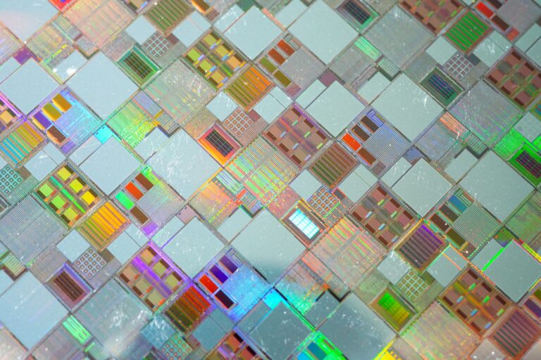
An integrated circuit (IC) is a set of electronic circuits miniaturised onto a single piece of silicon. A custom IC, more formally known as an Application-Specific Integrated Circuit (ASIC), is one designed to perform a specific function for a specific product, rather than a general-purpose component available on the open market.
For industrial applications, a custom IC is a device whose process technology, circuit architecture, and packaging have all been chosen to maintain reliable performance across the full thermal, mechanical, and electromagnetic envelope of the environment it will operate in, whether that is a factory floor, an outdoor infrastructure installation, or heavy industrial equipment running continuously in demanding conditions.
In practice, an industrial ASIC typically consolidates what would otherwise be multiple discrete components, integrating functions that previously required several circuits, passives, and connectors into a single device. Most industrial custom ICs are mixed-signal designs, combining analogue circuits that interface with physical sensors and actuators with digital circuits that process and communicate the data. For a deeper explanation of mixed-signal ASIC design, specifically, including the three main design categories and the engineering challenges involved, see our guide to mixed-signal ASIC design: applications, challenges and best practices.
Why Industrial Businesses Choose ASICs
The decision to pursue an ASIC is rarely made on a single factor. It is usually the combination of several requirements that standard parts cannot meet simultaneously. The most common drivers in industrial applications are:
Reliability in Harsh Environments
Commercial off-the-shelf components are designed for commercial operating conditions. Industrial environments are not commercial. Factory floors, outdoor infrastructure, heavy vehicles, and process plant equipment expose electronics to temperature extremes, vibration, shock, moisture, dust, and electromagnetic interference (EMI) at levels that will cause standard components to fail prematurely or behave unpredictably.
In practice, the risks are specific. Many industrial sensors generate signals with amplitudes of only a few millivolts, leaving very little tolerance for interference. Electrical noise from motors, switching power supplies, inverters and high-frequency drives can easily couple into these small signals and distort them.
When sensors are located away from the control cabinet, long cable runs increase vulnerability by picking up common-mode noise or creating ground loops, both of which can shift or obscure the true measurement before it reaches the processing electronics. An ASIC addresses this at the source, integrating amplification, filtering, and compensation into a single circuit optimised for the specific sensor type and environment.
An ASIC can be designed from the outset for the specific conditions it will face, with the circuit architecture, process technology, and packaging all chosen to maintain reliable performance in the required conditions.
Lower Power Consumption
For remote sensors, battery-powered IIoT devices, and edge processing nodes, power consumption is a competitive issue.
An ASIC is sized precisely for the signals and bandwidth it needs to handle, eliminating the excess current drawn by general-purpose circuits designed to cover a broad range of applications.
In deployments with thousands of nodes, the power saving per device translates directly into longer battery life, lower thermal management cost, and reduced operational costs across the network.
Smaller Product Footprint
Consolidating multiple discrete components into a single custom IC reduces the size and weight of the end product. For smart sensors, handheld industrial devices, and embedded controllers where board space is constrained, this is often the difference between a product that fits the application and one that does not.
When the sensor element itself also needs to be integrated, a System in Package (SiP) combines the MEMS sensor and the ASIC die into a single calibrated unit, reducing size further while removing calibration effort from the customer’s assembly line.
For more on how this approach is shaping industrial sensing, see how SoC and SiPs are at the heart of intelligent sensing.
Security and Intellectual Property Protection
In an ASIC, proprietary algorithms, calibration data, and signal processing logic are physically embedded in silicon, making the core intellectual property significantly harder to extract or reverse-engineer than in a software or discrete component-based design.
For industrial products where the sensing or processing method is a competitive differentiator, this level of protection is difficult to achieve with any software-based approach. Swindon Silicon designs with 100% IP protection as a baseline requirement, with no standard parts in the design that could expose the architecture.
Long Product Lifecycles
Industrial systems are often deployed for 10, 15, or 20 years. The components they depend on are not. Standard parts are regularly discontinued as semiconductor manufacturers shift their portfolios, and the consequences for industrial operators can be severe: emergency redesigns, production stoppages, or the need to stockpile years of inventory to avoid such eventualities.
An ASIC significantly reduces this exposure. The design is yours, the supply relationship is direct, and the product lifecycle is actively managed to run as long as possible.
Where end of life does eventually become unavoidable, as it can be when the underlying process technology reaches the end of its own life, a good supplier should support customers through that transition with structured options including last time buys and process transfers, rather than simply pulling the plug on a product line.
Common Industrial ASIC Applications

Custom IC design is applied across a wide range of industrial sectors and use cases. The most common industrial ASIC applications include:
- Smart sensors and IIoT devices: Mixed signal ASICs for precise sensor conditioning and real-time processing at the edge, integrating the full signal chain onto a single device to improve accuracy and reduce susceptibility to electrical noise. For a practical example, see our ASIC solution for low power industrial pressure sensing.
- Factory automation and robotics: Encoder ASICs for positional feedback in collaborative robots and automated assembly equipment, where measurement accuracy determines process repeatability.
- Motor drives and motion control: Custom circuits providing high-speed, precise drive electronics for motors, actuators, and piezoelectric systems where standard drive ICs cannot meet the timing or power requirements.
- Predictive maintenance systems: ASICs with integrated digital processing enable continuous, low-latency monitoring of machinery to detect wear or faults before they cause failures, reducing unplanned downtime and supporting safety monitoring in environments where early detection of hazardous conditions is as important as operational efficiency.
- Machine vision: High-speed optical image sensing ASICs for real-time inspection on production lines, where standard image sensors cannot deliver the combination of speed, resolution, and power envelope required.
- Power management and smart metering: Low-power custom ICs for energy harvesting, grid management, and intelligent metering infrastructure where efficiency and long-term supply assurance are both critical.
- Secure access and industrial identity: Dedicated processing blocks for cryptographic acceleration and secure communications in smart factory access and identification systems.
ASIC vs FPGA vs Off-the-Shelf: Which Is Right for Your Product?
The most important question in any custom IC evaluation is not whether ASICs are better than the alternatives in general, but whether they are the right choice for your specific industrial product, volume, and timeline. For industrial applications in particular, supply lifecycle and suitability for harsh environments often carry as much weight in the decision as unit cost.
FPGAs offer genuine flexibility at lower volumes and are often the right answer for industrial products that are still evolving or that will never reach the volumes needed to justify ASIC development.
It is worth noting, however, that FPGAs are predominantly digital devices and cannot fully replicate the analogue signal conditioning capabilities of a mixed signal ASIC, a consideration that is particularly relevant for sensor-driven industrial products where analogue performance is central to the design.
The point at which an ASIC typically becomes the better commercial choice for an industrial programme is when production volumes are high enough to amortise the upfront Non-Recurring Engineering (NRE) cost, when power or size constraints cannot be met by an FPGA, or when long-term supply lifecycle control is a hard requirement, as it frequently is in industrial systems deployed for a decade or more.
For a fuller look at how the two options compare across the product lifecycle, see our breakdown of ASICs vs FPGAs and the pros and cons of each.
The ASIC Design Process
An industrial ASIC programme moves through six stages. Understanding each one helps engineering managers plan realistic timescales and helps buying organisations understand where time and cost are concentrated.
- Define requirements. The full operating envelope must be captured before design begins: performance targets, interface protocols, supply voltages, temperature range, EMI environment, packaging constraints, qualification standards, and expected production lifetime. Changing fundamental requirements after tapeout is expensive. The quality of the requirements definition is the single biggest determinant of programme cost and timescale.
- Architecture and feasibility. The design team selects the process technology, determines the analogue, digital, or mixed-signal architecture, identifies existing, proven IP blocks that can be reused, and assesses the technical and commercial feasibility of the programme. A well-structured feasibility study at this stage de-risks the investment before any significant resource is committed.
- Design and verification. Circuit design, simulation, and rigorous verification across all process, voltage, and temperature corners. For mixed-signal industrial ASICs,this stage is both the most engineering-intensive and typically the most significant cost in the programme.. Simulation cannot catch every class of problem, which is why verification depth and the experience of the design team both matter significantly.
- Tape-out and manufacture. The completed design is submitted to a semiconductor foundry for fabrication. Tape-out is a major financial milestone in the programme, and managing foundry relationships, process selection, and design rule compliance carefully at this stage is critical to a successful outcome.
- Tape-out and manufacture. The completed design is submitted to a semiconductor foundry for fabrication. Tape-out is the point of highest financial commitment in the programme, and managing foundry relationships, process selection, and design rule compliance carefully at this stage is critical to a successful outcome.
- Production support and supply management. Long-term supply planning, quality assurance, and order fulfilment. For industrial applications with decade-long product lifecycles, this stage is as commercially important as the design itself. A full turnkey partner handles this under one roof, from initial specification through to the last shipment of the programme.
Our ASIC design flow sets out how each of these stages is structured in practice.
When Does an Industrial ASIC Make Commercial Sense?

For engineering managers, the feasibility question is whether the performance requirements can be met by a custom IC at an acceptable cost and within an acceptable timescale. For buying organisations and semiconductor managers, the question is whether the commercial benefits outweigh the development investment.
The upfront cost of a ASIC programme is driven largely by NRE, the one-time development cost that covers design engineering, simulation, verification, mask sets, and initial wafers. Unlike unit cost, NRE does not recur with each device produced, which is why the economics improve significantly at volume and over a long product lifecycle. For analogue and mixed signal designs, ASIC development costs have fallen significantly in recent years, making custom IC development accessible to a wider range of programmes than many assume.
The case is strongest when one or more of the following apply:
- Annual production volumes are high enough to amortise NRE cost, typically from hundreds of thousands of units per year upwards, though this depends on the unit price differential and the value of non-cost benefits.
- The product will be manufactured and supported for many years, making long-term supply control commercially valuable.
- Existing BOM costs are too high, and a ASIC can replace several discrete components with a single device at a lower unit cost.
- Reliability failures are costly, and standard components cannot be qualified to the required operating conditions.
- Power consumption is a competitive constraint that neither standard parts nor FPGAs can meet.
- The sensing or processing method needs to be protected as IP.
- A key component in an existing design is approaching the end of its life, and a controlled replacement is needed.
Obsolescence recovery is one of the most commercially straightforward cases for an ASIC. A standard part is being discontinued, redesigning around another standard part carries the same obsolescence risk again, and an ASIC solves the problem once.
Swindon Silicon designs replacement devices that are pin and functionally compatible with the original component, minimising disruption to existing production lines and removing the need for a full system redesign.
Common Mistakes to Avoid
Most ASIC programme failures or overruns can be traced back to a small number of avoidable mistakes:
- Starting design before requirements are stable. Incomplete or evolving specifications are the most common cause of costly programme changes. Investing time in a thorough requirements definition and feasibility study before circuit design begins is always the right approach.
- Underestimating verification effort. Verification typically consumes more engineering time than design in a well-run ASIC programme. Identifying problems in simulation rather than on silicon is significantly less expensive, which is why verification depth and rigour are worth investing in from the outset.
- Ignoring production test from the outset. The testability of the device and the cost per unit on the test floor are shaped by design decisions made early in the programme. Involving the test team at the specification stage avoids test coverage gaps and yields problems that can be difficult to resolve retrospectively.
- Choosing an ASIC too early for low-volume prototypes. For products that are still in early development, an FPGA can often provide the flexibility needed to evolve the design before committing to silicon. The ASIC decision should be made when the requirements are stable, and the volumes justify it.
- Selecting a design partner without production experience. Designing an ASIC and supporting it reliably at volume over a 15-year programme are different challenges that require different capabilities. When evaluating a partner, it is worth confirming that their design expertise is matched by established production infrastructure and long-term supply support.
In Summary
Custom IC design gives industrial businesses a meaningful edge through reliability, power efficiency, miniaturisation, IP protection, and lifecycle control that standard components and FPGAs cannot match. The upfront investment is greater, but for the right product and the right volumes, the long-term commercial returns are substantial.
The key is matching the decision to the right point in the product lifecycle, when requirements are stable, volumes justify the investment, and the programme has a partner who can support it not just through design but through decades of production.
Swindon Silicon has been designing and delivering custom mixed-signal ICs since 1978. As a full turnkey solution provider, the team supports programmes from initial specification through ASIC design, wafer probe, packaged test, quality assurance, and order fulfilment, all under one roof. With more than 1 billion ASICs in the field and 150 million die shipped annually, Swindon has the depth of experience and production scale to support industrial programmes where reliability and long-term supply continuity are not optional.
If you are evaluating whether a custom IC is the right solution for an industrial product, the starting point is a conversation about your requirements and whether the commercial case stacks up.
Contact the Swindon Silicon team to start that discussion.