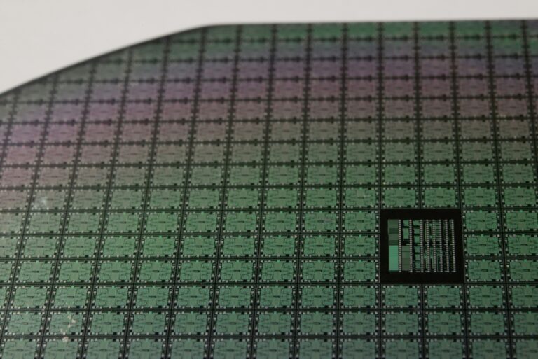
An application-specific integrated circuit (ASIC) solves a specific engineering problem that general-purpose semiconductors cannot. But between the initial concept and the finished die sitting on your production line lies a carefully orchestrated sequence of technical decisions, simulations, verifications, and physical fabrication steps.
This in-depth guide walks through the entire design-to-silicon journey: how engineers translate a system requirement into a working die, the choices they make at each stage, and the hand-offs and dependencies that shape the final result.
Stage 1: Defining Your ASIC Requirements and Feasibility
Every ASIC project begins with a core question: What problem are we solving, and will an ASIC actually solve it? This phase is about understanding the system, its constraints, and whether an ASIC is the right approach.
Feasibility and Architecture Review
The process starts with a feasibility study. As Ross Turnbull, Director of Business Development at Swindon Silicon Systems, explains:
“Designing an ASIC starts with analysing the target system, including identifying performance targets, power budgets, physical size constraints and interface needs. Engineers will carry out feasibility studies to assess whether the project is technically and economically feasible.”
Engineers analyse the target application, mapping out:
- Performance targets: speed, latency, throughput
- Power budgets: peak power, average power, standby
- Thermal and mechanical constraints: die size, package, heat dissipation
- Environmental operating conditions: temperature range, vibration, electromagnetic interference
- Interface and signal requirements: digital I/O, analogue inputs, communication protocols such as SPI or I2C
- Volume and cost targets: From 1 to 10K units per year and upward through high-volume production)
In parallel, architecture reviews explore multiple design approaches to the problem. Should the ASIC’s design be purely digital, mixed-signal (combining analogue and digital blocks), or memory-intensive? Should key functions be implemented as standard cells, or would a custom layout of a critical analogue block give better performance? What trade-offs between power, speed, die size, and cost are acceptable?
Creating the Design Specification
Once the architecture is chosen, a detailed design specification is written. This document becomes the contract between the system designer and the design team. It defines:
- Functional behaviour: what the ASIC must do
- Performance requirements: timing, signal integrity, and noise immunity
- Power consumption targets for each mode of operation
- Manufacturing and test requirements: which design rules apply and what test coverage is needed
- Supply, packaging, and longevity needs: single-source risk and end-of-life management
This specification phase is critical. Ambiguity or incompleteness here can cascade through the entire design and delay tape-out. Conversely, a clear specification enables the design team to move quickly and with confidence.

Stage 2: Design and Simulation
With the specification in hand, the design phase transforms requirements into a netlist, which is a detailed description of logic gates, transistors, and interconnections.
Using IP Blocks and Standard Cells
Rather than designing every function from scratch, the design team often draws on proven intellectual property (IP) blocks and standard cells from the foundry’s process library. For example:
- Analogue IP blocks: precision voltage references, amplifiers, and analogue-to-digital converters (ADCs)
- Digital IP blocks: multipliers, memory compilers, and I/O buffers
- Standard cells: logic gates, flip-flops, and other primitives optimised for the target process technology
These pre-verified, tested building blocks accelerate design and reduce risk.
Mixed-Signal Design Considerations
For a mixed-signal ASIC (which combines analogue and digital subsystems), the design phase must address the interaction between the two. Noise from the digital core can couple into sensitive analogue circuits. Clock signals must be routed carefully. Power supply distribution must be designed to avoid ripple that would corrupt analogue measurements. The design team uses specialised layout and simulation techniques to manage these challenges.
Simulation and Corner Analysis
Throughout the design phase, engineers run simulations to verify behaviour:
- Functional simulation: Does the logic do what the specification requires?
- Timing simulation: Do signals arrive when expected, or is there slack/violations?
- Corner simulations: How does the design behave at the extremes of temperature (−40 to +125 °C in grade 1 automotive), supply voltage, and manufacturing process variation?
- Power analysis: Is power consumption within budget?
- Signal integrity and noise analysis: Is noise budget adequate?
These simulations iterate. If specification is violated, the design team might increase gate sizes, reorder logic, or adjust clock distribution. Each iteration narrows the design toward a solution that meets all constraints.
Stage 3: Physical Design, Custom Layout, and Optimisation
Simulation verifies behaviour in theory. Physical design brings it into reality.
Logic Synthesis and Placement
Starting from the verified netlist, automated tools synthesise the design into a gate-level netlist using the foundry’s standard cell library. For most designs, place-and-route is heavily automated. For others (particularly analogue circuits, high-frequency digital blocks, or performance-critical paths) custom layout is applied.
Custom Layout and Optimisation
Custom layout is where a designer places transistors with nanometer scale precision, routes signals to minimise parasitic capacitance, and arranges power delivery to maintain voltage uniformity. Custom layout unlocks performance unavailable through automated place-and-route. It entails:
- Analogue blocks: Differential pairs in precision amplifiers must be physically matched to within a fraction of a micron
- High-speed digital: Critical timing paths might be hand-routed to minimise wire delay
- Power delivery: In high-current blocks, custom power mesh design reduces voltage droop
Custom layout can add cost and schedule, so it is typically applied only where the performance gain justifies it.
Design Rules and Verification
Throughout layout, the design must obey the foundry’s design rules. Automated design-rule checking (DRC) catches violations, which are then corrected.

Stage 4: Verification and Validation
Before the design ever enters fabrication, it undergoes rigorous verification to catch errors early.
Full-Chip Verification
At this stage, the complete design is verified to ensure functional correctness, electrical correctness, timing correctness, and electrical rule checking (ERC).
Test Plan Development
Detailed test plans are developed for use after fabrication:
- Wafer probe test: A parametric test performed on the die before packaging
- Automated test equipment (ATE) test: Used after packaging to verify functional performance
These test plans go hand-in-hand with design. Scan chains (serial shift registers that make internal signals observable during testing) are added to digital blocks. This enables efficient, comprehensive test coverage and observability of internal signals.
ASIC Qualification Testing Preparation
For automotive, industrial, or aerospace ASICs, qualification testing is mandatory. During design, the design team prepares detailed specifications for the qualification tests. Qualification tests can include:
- Tri-temperature testing
- Burn-in testing (extended operation at elevated temperature and voltage)
- Electrostatic discharge (ESD) robustness
- Electromagnetic compatibility (EMC)
These tests are typically carried out after tape-out, but their requirements are designed-in during this phase.
Stage 5: Tape-Out and Fabrication
“Tape-out” is the moment the design is locked and sent to the foundry for fabrication. The term persists from the era when designs were recorded on magnetic tape.
Design Handoff to Foundry
A complete design package includes the GDS-II file, verification reports, test specifications, design documentation, and fill patterns. The foundry checks that the design meets all its requirements before committing to the fabrication schedule.
Photomask Generation and Fabrication
The foundry creates photomasks: the templates used to etch each layer of the die. Mask-making often takes one to two weeks. Fabrication itself takes eight to sixteen weeks, depending on process complexity and factory throughput.
Engineering Samples and Prototyping
Once fabrication is complete, the next steps depend on the project structure. For some products, wafer probe testing is performed on the die while still on the wafer, providing rapid feedback before packaging. For others, a selection of die are packaged first, then tested post-package.
The number of available engineering samples depends on wafer yield and the quantity of die per wafer. For most projects, this provides sufficient devices for design validation and customer prototyping. However, in multi-project wafer (MPW) runs the number of available die is very limited, since die are allocated across all projects on that wafer. At this stage, the design team performs functional testing and parametric characterisation, and prototyping begins with the customer.

Stage 6: Design Refinement and Sign-Off
Based on characterisation data and customer feedback from engineering samples, minor adjustments might be needed. In some cases, simple metal-layer changes can be made without re-spinning the entire design.
Once all data confirms the design meets specification, the design team signs off, and the project moves into production release and beyond-design phases (test, quality, lifecycle management). For more detail on these stages, see our article on ASIC test, quality, and lifecycle management.
Whether you are designing next-generation automotive control systems, industrial automation platforms, or aerospace sensor networks, a discussion with an experienced ASIC design partner can help you navigate feasibility, confirm realistic timelines, manage costs, and ensure your custom IC is designed for manufacturability and long-term reliability.
Swindon Silicon brings 40+ years of expertise in mixed-signal design and deep knowledge of ASIC design-to-silicon delivery. If you are considering whether an ASIC could benefit your application, contact our experts.