The moment an ASIC design is complete and ready for fabrication is not the finish line. It is the start of a new and equally critical phase: testing, quality assurance, and long-term lifecycle management. This phase determines whether a device that works in simulation will perform reliably in the field, and whether it will remain available when customers need it months, years, or even decades later.
This article explores what happens after the design phase, from the earliest testability decisions through qualification, production testing, and the proactive lifecycle management that protects customer investments over the long term.
Design for test (DFT): building quality in from the start
Quality in semiconductor manufacturing must be designed in from the beginning. This principle translates to ASIC design as design for test (DFT): a set of architectural and circuit-level techniques that make a device easier to test and enable comprehensive detection of manufacturing defects before devices are ever shipped.
Why DFT matters
The silicon from a foundry is not delivered pre-tested. After fabrication, each die on a wafer must be electrically tested to ensure it was manufactured without defects. Without DFT, achieving high test coverage (the percentage of potential faults that can be detected) becomes expensive and slow. DFT allows test patterns to be generated automatically, applied efficiently using automated test equipment (ATE), and executed at high throughput. This directly impacts both quality and cost.
DFT as a design trade-off
Adding DFT structures (extra multiplexers for scan insertion, BIST circuitry, and test points) introduces area overhead (typically 5 to 15% of total die area) and modest power overhead. However, for applications where field failure costs are high and long-term reliability matters (such as industrial, aerospace, or automotive applications), this overhead is a worthwhile investment. For consumer products with different cost-margin constraints, the trade-off may be different. Your ASIC partner will often discuss DFT trade-offs during the specification phase to find the most suitable option for each use case.
ISO 9001 and quality management systems: the foundation for consistent quality
Quality emerges from processes that are defined, followed, audited, and continuously improved. This is the purpose of a quality management system (QMS). The international standard that governs it is ISO 9001.
What ISO 9001 means
ISO 9001 is a framework standard published by the International Organisation for Standardisation. It sets out the organisational and process requirements that a company must implement to ensure consistent quality across design, manufacturing, test, and supply operations.
An ISO 9001-certified organisation must:
- Document all processes
- Maintain traceability
- Control suppliers
- Implement internal audits
- Demonstrate continuous improvement
- Manage customer feedback
An ISO 9001 certification is a useful signal: it means the company has undergone a rigorous third-party audit and is regularly reviewed for compliance.
A supplier operating under ISO 9001 can typically also confidently provide the evidence that engineering teams and procurement need to justify their choice to internal stakeholders.
Production test: catching defects at scale

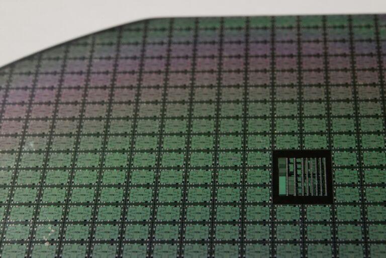
Once silicon is fabricated at the foundry, it arrives as a wafer containing hundreds or thousands of dies. Before these dies are ever packaged, they undergo electrical testing in a process called wafer probe or die sort. After packaging, they undergo a second round of testing: final test or packaged test. Together, these two test stages form the production test regime that ensures every device has been verified as functional.
Wafer probe: the first gate
Wafer probing occurs while dies are still on the wafer, before dicing and packaging. A wafer prober contacts the electrical pads of each die with microscopic needle probes. These probes establish temporary electrical connections to the die, allowing test signals to be applied and responses to be measured. Any dies that fail the wafer probe test are marked and later mechanically separated during dicing. Only passing dies proceed to packaging.
Wafer probe coverage typically includes:
- functional tests (does the logic behave correctly?)
- parametric tests (are voltages, currents, and timing within specification?)
- DC tests (are there any short circuits or leakage paths?)
Packaged test: final verification
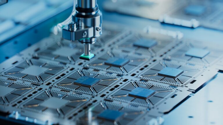
After packaging, devices undergo a second round of testing in the final test. The packaged test uses automated test equipment (ATE) connected to the device via a test socket or probe card. The ATE applies test vectors, measures responses, and compares them against expected results.
Final test serves several purposes:
- Package integrity: The packaging process (the heating, cooling, and mechanical stresses involved in assembly) can damage dies or create electrical faults. Final test verifies the device still works correctly after packaging.
- Temperature characterisation: Final test equipment is often equipped with temperature chambers, allowing devices to be tested at minimum, nominal, and maximum operating temperatures. This verifies that the device meets its specification across its full temperature range.
- Additional parametric testing: Measurements like quiescent current (IDD), supply voltage sensitivity, and timing characteristics are recorded and used to screen out marginal devices.
For high-reliability applications, devices may undergo multiple temperature testing steps to ensure robust parametric performance.
Test coverage and defect detection
The effectiveness of production test depends on how well the test vectors exercise the device and how high the fault coverage achieved. With DFT properly integrated into the design and test coverage at or above 95%, the production test regime can detect >99% of manufacturing defects. This is why DFT and production test are inseparable: good DFT enables efficient, comprehensive testing.
The cost per test is often measured in fractions of a cent per device. The value of catching a defect in the factory (where it is discarded) versus in the field (where it causes a customer failure) is orders of magnitude higher. This is why production test rigour directly translates to field reliability.
Burn-in and infant mortality screening
In any population of manufactured devices, a small percentage contain latent defects: manufacturing flaws that do not cause immediate failure but are unstable and will fail when stressed. This phenomenon is captured in the reliability ‘bathtub curve’: early failures (the infant mortality region), random failures (the useful lifetime), and wear-out failures (the end of life).
Burn-in testing is a screening technique that subjects devices to stress conditions such as elevated temperature and elevated voltage to force latent defects to manifest as actual failures. Only devices that survive burn-in proceed to the customer. This significantly reduces the field failure rate in the early operating period.
The data from burn-in testing (the number of devices that fail and when during the burn-in period) is used to estimate the field failure rate. This data informs the reliability model and allows suppliers and customers to assess whether the early failure rate is acceptable.
Reliability qualification: proving long-term performance
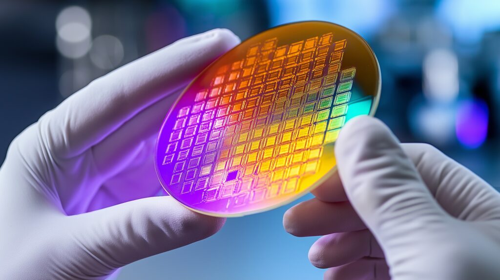
Reliability qualification testing asks: will this device continue to function correctly after years of operation in its intended environment?
Reliability qualification is where the ASIC investment pays dividends. An ASIC designed and qualified for a specific application can be proven reliable under its actual use conditions in ways that off-the-shelf components often cannot match. The qualification test plan, grounded in JEDEC standards and tailored to the application, provides the statistical evidence needed to predict long-term field performance with confidence.
For more information on specific qualification methods and the standard governing them, read our blog on ASIC reliability qualification.
What qualification data reveals
The outcome of a well-executed qualification programme is a set of failure mode data, a reliability model, and evidence that the design has adequate margin across its operating envelope.
When a supplier presents qualification data showing that an ASIC passed 1,000 hours of HTOL (High Temperature Operating Life) testing at 125°C with zero failures, a 168-hour HAST (Highly Accelerated Stress Test), 500 thermal cycles, and robust ESD (Electrostatic Discharge) performance, they are providing the empirical foundation for a long-term reliability claim. Customers can review this data and make informed decisions about whether the demonstrated reliability matches their application needs.
Conversely, if qualification testing reveals failures, the data also reveals where the design is weak. This can drive design changes such as adding derating, changing materials, redesigning circuits for robustness before production release. Failures in qualification are valuable because they are found early, when design changes are still feasible.
Supply assurance and lifecycle management: planning for the long term
Supply continuity and proactive lifecycle management are integral to the value proposition of an ASIC.
The lifecycle mismatch problem
Modern semiconductor components typically remain in production for 5 to 10 years before being discontinued as market demand shifts and manufacturing focus moves to next-generation products. In contrast, industrial, automotive, and aerospace systems are often designed for service lives of 15 to 30 years, and spare parts obligations may extend even longer.
This mismatch creates a structural challenge: a system designed to operate for 20 years will almost certainly outlive the initial availability of its semiconductor components. Without proactive management, an EOL (end-of-life) notification can force costly redesign or supply chain workarounds.
Proactive lifecycle management versus reactive obsolescence
Two approaches exist in response to this: reactive (waiting for an EOL notice, then scrambling to respond) and proactive (anticipating obsolescence and planning transitions in advance).
A good ASIC supplier adopts a proactive approach. This means:
- Monitoring component status: The supplier tracks the status of every process technology and foundry partner used in production, maintaining awareness of which nodes are maturing and which are approaching EOL.
- Planning ahead: For ASICs approaching the EOL phase, the supplier engages customers in advance to discuss options.
- Last-time buy planning: When an EOL notice is inevitable, the supplier and customer work together to estimate total demand (production volumes plus service/repair demand) and determine the appropriate last-time buy quantity. This may mean placing a large order months before the formal EOL date, securing inventory that will support the customer through the remainder of the product lifecycle.
- Process transfer evaluation: For products requiring long-term support, the supplier may evaluate whether the ASIC design can be transitioned to a more modern process node, offering the customer a path to continued supply without a complete redesign. A well-architected ASIC, with careful attention to power and performance requirements, can often be ported to a newer node.
As Ross Turnbull, Director of Business Development at Swindon Silicon Systems, explains:
“As ASICs are designed specifically for the application they will support, designers can replicate the functions of an obsolete component or surpass its performance. In addition to supporting obsolescence recovery, ASICs deliver a host of benefits for manufacturers, including higher performance, lower power consumption, a smaller footprint, a reduced bill of materials and improved reliability.”
The competitive advantage of proven quality and supply assurance

In markets where reliability matters and long-term supply is critical (such as industrial automation, automotive, aerospace, and medical devices), the ASIC supplier’s test and lifecycle capabilities are often more important than design brilliance.
A clever design that is poorly tested or discontinued without notice can be a liability. By investing in comprehensive DFT, rigorous qualification testing, robust production quality control, and proactive lifecycle management, an ASIC supplier distinguishes itself as a dependable partner. For procurement and quality teams evaluating suppliers, these qualities should weigh heavily in the decision.
Swindon Silicon operates to BS EN ISO 9001 standards and has test infrastructure for HTOL, HAST, burn-in, ESD and thermal cycling. They actively manage obsolescence risk with structured planning, last-time buy support, and process transfer capabilities where feasible. These capabilities are embedded in how Swindon Silicon engages with every customer and every programme.
If you are specifying an ASIC for an application where reliability, test rigour, and supply longevity are critical, contact Swindon Silicon Systems to discuss how comprehensive test and lifecycle management can be embedded in your programme.